Gallium Arsenide Impurities Change Optical Properties
Published on Fri Jan 19 2024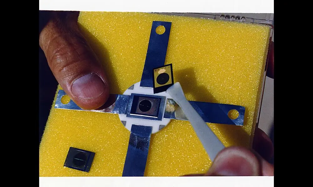 197 007 005 | U.S. Department of Energy on Flickr
Gallium arsenide (GaAs), a star in the semiconductor world, has yet again grabbed the spotlight in a new study revealing the intricate dance of absorption within its structure, which could influence the future of optical and electronic devices. Researchers from the Bangladesh University of Engineering and Technology have taken a deep dive into understanding why and how GaAs deviates from the ideal when it comes to light absorption. Their findings, strikingly elaborated on through numeric analysis, shed light on the impact of additional energy states caused by impurities and defects that often appear in semiconductor materials.
At the heart of their investigation is the absorption coefficient of GaAs, a direct measure of how strongly a material can absorb light at different energies. Normally, the absorption spectrum of a semiconductor like GaAs is smooth and predictable; however, the real world isn't perfect. Imperfections within the crystal structure, such as vacancies and impurities, introduce unexpected energy states leading to variations in the material’s absorption characteristics. These deviations can alter how efficiently GaAs absorbs and emits light—a critical factor for applications ranging from solar cells to laser diodes.
The researchers meticulously analyzed how variations in the density and energy levels of these imperfections affected the absorption coefficient. Surprisingly, even the smallest density of 2% could cause noticeable deviations, particularly when impurity states were further away from the main conduction band of the GaAs. In practice, this means that even minute differences in material purity can have significant impacts on the performance of GaAs-based devices.
This study has practical implications, offering a compass to navigate the complexities of impurity levels and energy state densities within GaAs. The detailed absorption spectra crafted by the researchers could serve as a blueprint for engineers aiming to measure and minimize the imperfections in these powerful semiconductors, leading to more precise and efficient optoelectronic devices. As we push the boundaries of what's possible with technology, such insights become invaluable in refining the materials that will power the next generation of electronics and photonics.